Resonac Accelerates Semiconductor Materials Development with AI-Based Cutting-Edge Simulation Technology
-First elucidation of the semiconductor substrate polishing mechanism using CMP slurry through calculations made 100,000 times faster yet with accuracy-
August 06, 2024
Resonac Holdings Corporation
Resonac Corporation (President: Hidehito Takahashi, hereinafter “Resonac”) is introducing neural network potential (NNP) technology, a new simulation technology that combines the first-principles calculation method commonly used in simulations for material development and artificial intelligence (AI) to simulate and elucidate the semiconductor circuits polishing mechanism using CMP slurry*1.This technology is the first of its kind in the world.*2 NNP technology is capable of the previously difficult feat of simulating chemical reactions more than 100,000 times faster while maintaining the same level of accuracy as first-principles calculations. This technology will enable Resonac to elucidate the behavior of materials occurring in the complex semiconductor fabrication process and rapidly create new materials.
Recently, the speed of technological innovation in the semiconductor industry has been accelerating, and there is a need to provide new materials quickly. Efforts are underway to accelerate the creation of new materials through efficient research and development by conducting experiments after simulation for rough estimation. For semiconductor fabrication processes, however, it is necessary to calculate the interactions at interfaces between materials with different properties, such as inorganic, metallic, and organic materials. In these cases, first-principles calculations are commonly used. While this method can produce highly accurate calculation results, calculations consume a large amount of time and computing power. It is therefore difficult to simulate mechanisms while taking into account complex chemical reactions and the surrounding environment, such as pressure. In addition, the limited reaction time available for analysis makes first-principles calculations unsuitable for semiconductor materials. Among them, the polishing process of semiconductor circuits using CMP slurry, which is crucial for semiconductor manufacturing, involves the presence of many molecules and atoms such as additives and abrasives. Additionally, it requires fine control of the complex geometry of the substrate, necessitating large-scale simulations both temporally and spatially.
For several years, Resonac has been studying the introduction to semiconductor materials development of NNP technology, in which the performance of AI has been dramatically improved by using AI semiconductors.*3 This state-of-the-art NNP technology allows us to train the AI model with tens of millions of data points from first-principles calculations and perform large-scale simulations with a high degree of accuracy comparable to first-principles calculations. With NNP technology, calculations that would take more than 1,000 years with first-principles calculations can be completed in 100 hours.
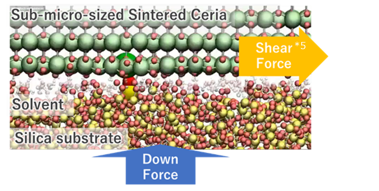
Resonac adopted state-of-the-art NNP technology to simulate the polishing process of semiconductor substrates using CMP slurry. As a result, Resonac successfully visualized complex interface behavior precisely on a nanometer*4 scale, allowing us to understand intricate polishing mechanisms that are difficult to capture through experiments alone.

By clarifying the process in detail, including the effects of the surrounding environment such as substrate geometry and processing conditions, we can find raw material candidates that produce the desired functions with a higher degree of accuracy. As a result, the development time for new materials can be shortened significantly.
NNP technology is effective for complex analyses of interfaces and heterogeneous mixtures, and Resonac has also applied it to semiconductor materials field other than CMP slurry.
Dr. Yoshishige Okuno, Head of the Research Center for Computational Science and Informatics, said,
“NNP is a new AI-based technology that allows us to perform more advanced materials analysis and discover new materials and raw materials by utilizing cutting-edge computational science and technology. I really feel that we are now in an exciting era in which we can utilize computers with AI semiconductors to perform AI-based simulations and thereby develop even better AI semiconductors”.
*1 A planarization polishing material for semiconductor integrated circuits. CMP stands for chemical mechanical polishing. Slurry is a water-based abrasive, consisting of abrasive grains and an aqueous solution. Depending on the surface material of the wafer to be polished, several types of slurries are used, such as ceria slurry and silica slurry. Slurry has become an essential material in the fabrication of today's highly integrated semiconductor devices, because surface planarization allows for the multilayering of circuits.
*2 Based on Resonac’s research (As a result of a survey on papers applying NNP to CMP slurry mechanism analysis, as of July 2024.)
*3 Graphics processing units (GPUs), also known as AI semiconductors, are processors with advanced matrix-computing capabilities, and are essential for high-speed, large-scale data processing and simulation, such as AI and NNP technology. The introduction of GPUs has made it possible to achieve much higher processing speed and efficiency than with conventional calculation methods.
*4 One billionth of a meter.
*5 Shear force is the force that causes parallel displacement within an object. It can lead to deformation or destruction of the object.
For further information, contact
Media Relations Group, Brand Communication Department
