WITH UNSUNG LEADERS -Stories of behind-the-scenes leaders who take on challenges for a better future-
Prof. Kuroda of the University of Tokyo and Resonac Think About Human Resources Necessary for the Semiconductor Industry
February 13, 2023
Semiconductors made in Japan accounted for more than half of the world market share in sales in the 1980s, but then followed a downward trend, and are now in the single-digit percentage range. Lagging behind the high-performance advances in South Korea, Taiwan, and the United States, the Japanese semiconductor industry, which has been facing headwinds for nearly 40 years, is now starting to see a tailwind. At the center of this trend is Prof. Tadahiro Kuroda, who launched the Systems Design Lab (d.lab) at the University of Tokyo in 2019.
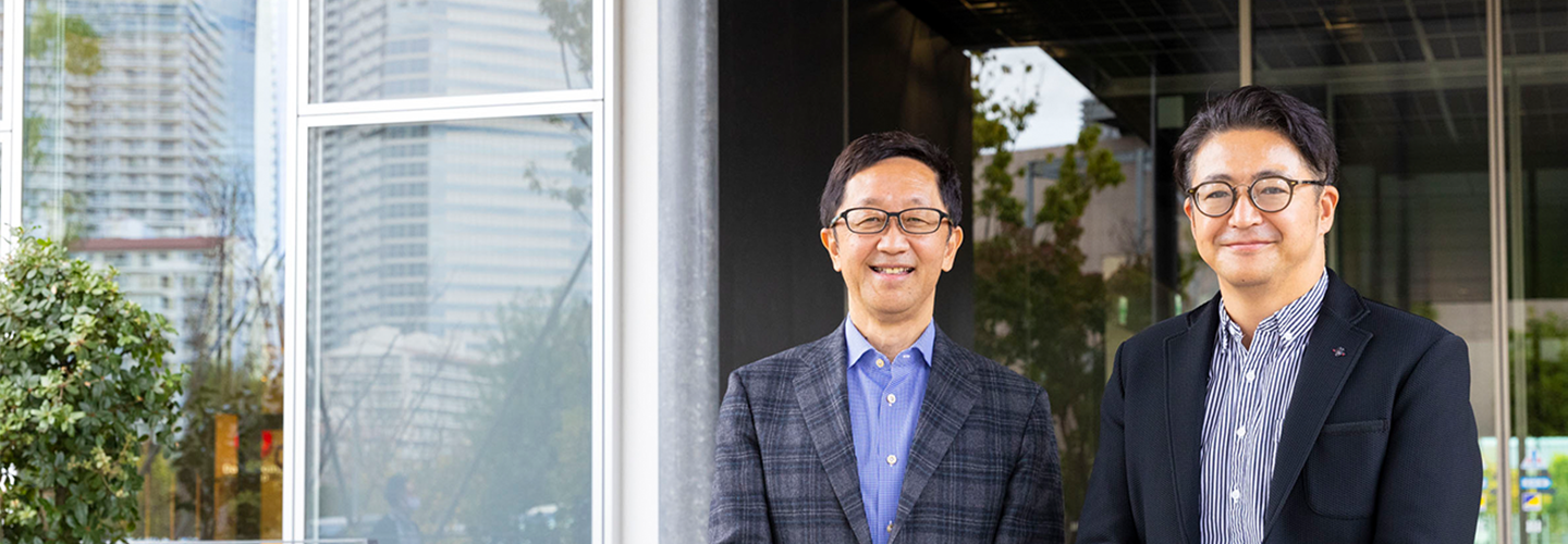
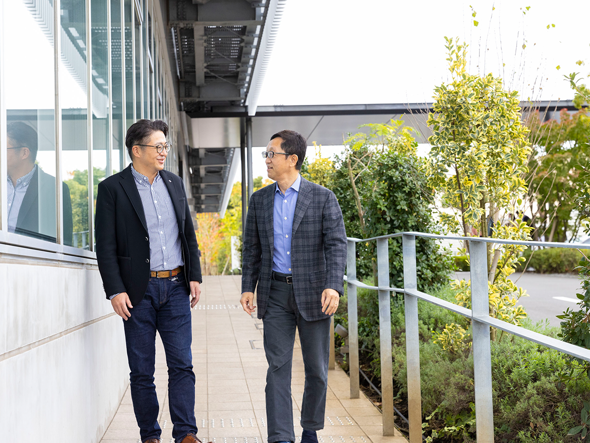
Prof. Kuroda works on the development of next-generation semiconductors through industry-academia collaboration under the slogan of “democratization of semiconductors,” while Hidenori Abe, Head of the R&D Center at Resonac’s Electronics Business Headquarters, leads the development of semiconductor packages with the keyword “co-creation.” In this two-part article, we interviewed them about the future of Japanese semiconductors and the human resources that the industry will require in the future.
What Is Required Is “Breadth of Vision” and “Communication Skills”
In Part 1, we heard about the background of the increasing importance of the “post-process” in semiconductor development and the need for a “forest of co-creation” for the development of next-generation packages. In Part 2, please tell us about the type of human resources that the industry is looking for.
Kuroda: It is difficult for a single company to develop semiconductors, which can be said to be the crystallization of state-of-the-art technologies in various fields. That’s why I talked about the need for collaboration that transcends corporate boundaries in Part 1. I called the open innovation space for that purpose a “forest of co-creation,” likening it to biodiversity, and “breadth of vision” and “communication skills” are important in the forest of co-creation where various human resources gather.
Abe: That’s even more true in the packaging process, where total optimization is now required. For example, there are cases where a material that has excellent electrical properties and is considered to be the best on its own cannot be used because the chip as a whole cannot withstand the heat generation. I think that in the future, post-process researchers will need to actively communicate with engineers in each area, including the pre-process, and proceed with development while considering the overall balance.
Kuroda: Semiconductors are no longer just transistors, but rather “big systems.” The academic fields necessary for the development of semiconductors are also expanding. In the old days, it would have been enough for engineers to just delve deeply into their areas of expertise, but today that stance no longer works. We have to be more outward-looking.
Abe: What’s more, it’s not enough just to be knowledgeable about technology and science. It’s also important to have the ability to create networks with various people and foster a forum for discussion.
Although we are based in Japan, most of our customers are overseas manufacturers. A higher level of communication skills is required in order to understand the direction in which overseas customers are heading and to draw a roadmap together with them.
Kuroda: In terms of regional characteristics of the industry, the semiconductor manufacturing market used to be centered in the United States, but now the center has shifted to Asia. Key players are very close to each other in Asia, and there is almost no time difference between Japan, Taiwan, South Korea and coastal China. Moreover, TSMC (*1) is building a new factory in Kumamoto, aiming for completion in 2024, and I think Kyushu was chosen because of its good access to other Asian countries and its advantages in terms of transportation.
- *1 TSMC (Taiwan Semiconductor Manufacturing Company Limited): The world’s largest semiconductor contract manufacturer (foundry) headquartered in Taiwan. Its global share of the semiconductor manufacturing market is more than 60%.
Considering these facts, I feel that a very good wind is beginning to blow in Japan today. The Japanese government announced that it will make a large-scale investment in the semiconductor field, and TSMC, the world’s largest foundry, was invited to set up a factory here, and geographically, Japan is located at the center of the global market. The soil for the revival has been prepared, so all we need now is human resources. The next 20 years should be a wonderful era for the Japanese semiconductor industry if we can create an environment where more diverse human resources can play an active role.
The First Step in Securing Human Resources Is to Present a Vision
What is the state of the world in terms of talent for the semiconductor industry?
Kuroda: Countries are competing for talented people. Behind this is the division of the world triggered by the confrontation between the United States and China. Each country has positioned semiconductors as the cornerstone of economic security and has the desire to manufacture them in their own country or to secure a stable supply in cooperation with allies. Along with this, the rush to retain excellent human resources has begun.
Does Japan also have a shortage of human resources?
Abe: In Japan, in addition to the declining birthrate, the decrease of science students is continuing, and so the number of people entering the semiconductor industry was also decreasing.
On the other hand, the growth rate of the semiconductor market is predicted to be very high in the future. Our semiconductor materials business is also expected to grow at an average annual rate of around 10%, and we believe that we will need a considerable number of engineers to continue business expansion. In the future, there will be a further shortage of engineers in the fields of manufacturing, design, and equipment, as well as materials.
Kuroda: Human resources are closely related to industry. Without human resources, industry will not become stronger, and without industry, human resources will not become richer. The challenge is how to develop excellent human resources in this dilemma, and this is a major theme the Japanese semiconductor industry is facing. Currently, the country is starting large-scale investment in the semiconductor field, but I would like to see continuous investment in human capital as well.
What can companies do to secure talent?
Kuroda: If you prepare rich soil where diverse human resources can play an active role, people will naturally come together and grow. So how do you prepare such rich soil? What’s important is having a “vision.”
When you try to start something new, there is usually a lot of opposition. When Taiwan’s TSMC was established, many people were surprised and negative, saying, “There is no way a foundry business will succeed.”
However, TSMC gradually struck a chord with many people and grew into one of the world’s leading companies by continuing to present a vision for a new business model, without being constrained by past successes or common sense. Currently, Resonac is also continuing to send out a strong message and vision, isn’t it?
Abe: We are conscious of that. Most customers who visit the Packaging Solution Center for the first time are surprised, asking, “Why does a materials manufacturer have so much equipment?” or “What are you guys aiming for?” We get those kinds of questions all the time.
And when we do, we explain our vision, saying, “Our company is focusing on packaging, but there is a limit to what one company can achieve, so we will continue to promote co-creation.” People emphasize with this. Sharing a vision is essential for promoting co-creation. By leading with a clear vision and operating the Packaging Solution Center as an open space equipped with an evaluation platform for cutting-edge packaging, we believe that we will contribute to the technological innovation of semiconductors.
The Future of the Semiconductor Industry Is Bright
Please tell us about your thoughts on human resource development from the perspective of industry-academia collaboration.
Kuroda: The other day, when I attended an international conference, there was a panel discussion on human resources. Deans from Arizona State University and other regions where semiconductor investment in the United States is active gathered to discuss the theme, “What we want industry to do.” The conclusion was, “We want industry to provide more good internship programs than ever before.”
They said, “We would like to see internship programs that take the educational aspect into consideration, in which the entire internship does not consist of letting the intern work on the sidelines, but where they really work together with professionals.” I thought that this is also necessary in Japan today.
Abe: Why was such an internship not possible until now? It’s probably because the company doesn’t want to openly disclose development information. However, the Packaging Solution Center is working on cutting-edge technology development in an open environment.
I think it’s a very attractive environment for students, so in the future, we will consider using it for more practical internships. Even if they don’t end up joining Resonac, we’ll be happy if they become interested in semiconductors.
In reality, how popular is the semiconductor industry among students?
Kuroda: For the last 20 years, it has been in a slump, but recently it has become more popular. One student graduated from my institute and got a job at TSMC. When I asked the student, “Why are you going to TSMC?”, they replied, “Because I can work with the world with cutting-edge technology. It’s exciting, and the salary is high too.” Conversely, I felt it was a little regrettable that Japanese companies are not yet providing such an environment, but it’s great to see an increasing number of young people aspiring to work in the industry.
Abe: We have to take a hard look at ourselves as well. These days, even if someone joins a company as a new graduate, they will quit as soon as they think, “This isn’t a place where I can grow.” I fear that unless we continue to provide an attractive work environment and prevent the outflow of human resources, the company will eventually cease to exist.
Personally, I think there is no other industry that is so huge, and that technology is evolving at such a tremendous speed. And so, I would like to convey the attractiveness of the semiconductor industry to the students. I would like to spread the message that the future of semiconductors is bright.
Finally, please give a message to young people who hope to join the semiconductor industry.
Kuroda: Let’s all create a “forest of co-creation” where various players in the semiconductor industry develop together. To do that, what we need is people with a broad perspective who are willing to live together and evolve together. Until now, human resources have been concentrated in the pre-process area, but from now on, post-process and packaging will also be an exciting area that requires advanced academics. I would love for you all to join us.
Abe: In recent years, the semiconductor materials industry has been globalizing at an accelerated pace, and the Packaging Solution Center is developing world-leading, cutting-edge technology in this field. If you want to experience the latest technology and take on new challenges, please come to Resonac. We’ll evolve together while having discussions with excellent people from many companies. Let’s open up the next era together in an environment unlike any other in the world.
In Part 1, we asked about the background of the increasing attention toward the post-process, which is key to the revival of the Japanese semiconductor industry, and the importance of collaboration that transcends companies, such as “co-creation” and “open innovation.”
Tadahiro Kuroda
Prof. Kuroda received his PhD in Engineering from the University of Tokyo in 1982 and joined Toshiba Corporation the same year. He was a visiting researcher at the University of California, Berkeley, from 1988 to 1990. He became an associate professor at Keio University in 2000, a full professor in 2002, and professor emeritus in 2019. He was the Mackay Professor at the University of California, Berkeley, in 2007. He became a professor at the University of Tokyo Graduate School and the director of System Design Lab (d.lab) in 2019, and the chairperson of RaaS in 2020. He has published over 300 papers, including 60 invited lectures and 30 books, and holds more than 200 patents. He has served as a member of the IEEE SSCS Administrative Committee, an IEEE Distinguished Lecturer, an IEEE/SSCS Region 10 Representative, and committee chair of A-SSCC. He is an IEEE Fellow, an IEICE Fellow, and committee chair of VLSI Symposia.
Hidenori Abe
General Manager of the Electronics Business Headquarters R&D Center, Resonac Corporation
After joining Hitachi Chemical Co., Ltd. in 1998, Abe was involved in the development of semiconductor sealing materials. He worked in the U.S. office for seven years and gained experience in technical services while obtaining an executive MBA. He was later involved in the establishment of the Packaging Solution Center and served as corporate marketing manager and the department head of the CMP slurry business. Currently, Abe is focusing his efforts on the development of overall semiconductor materials and related products, while promoting co-creation activities based on the Packaging Solution Center.