- Category:
- Tag:
Applicable Business AreasRF module manufacturers
Target ApplicationsRF module substrates
Applicable Business AreasRF module manufacturers
Target ApplicationsRF module substrates
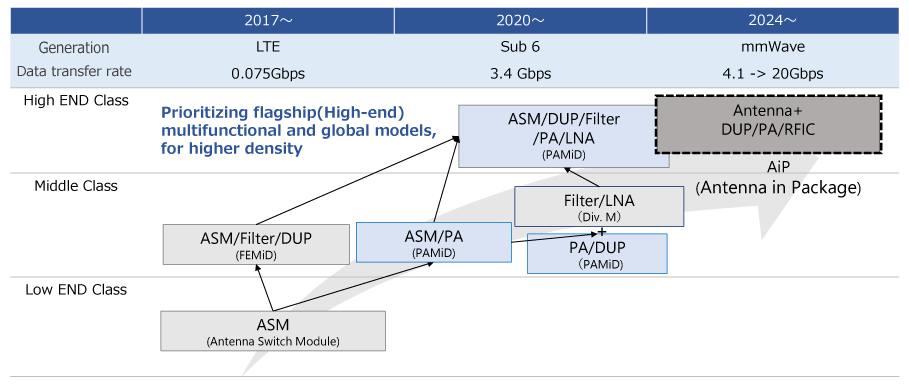
Wireless communications are advancing from 5G to 5G-Advanced and Beyond 5G (6G) in pursuit of higher speeds and larger capacity. To keep pace with these growing needs, smartphones and other mobile devices contain a burgeoning number of radio frequency (RF) communication chips, including amplifiers and filters, to handle multiple radio frequency bands and radio waves such as Bluetooth, Wi-Fi, and near-field communication (NFC). Accordingly, RF chips are increasingly modularized, with chips mounted in close proximity on a single substrate, while demand rises for highly integrated RF chips with chip-to-chip signals transmitted much faster in wider bandwidths. Space saving through modularization also helps equip smartphones with multiple functions, such as high-performance cameras and various types of sensors.
RF module substrates require low dielectric properties (low dielectric constant (Dk) and low dielectric loss tangent (Df)) with low transmission loss at high frequencies as well as low coefficients of thermal expansion (CTE) to ensure reliability.
Bismaleimide triazine resins are commonly used to produce these substrates. However, smaller RF modules are essential to create more space in response to expanding frequency bands and smartphones’ multifunctional capabilities. Multilayering with thinner substrates is an effective way to meet these demands, and substrates must also provide a lower Dk than conventional models.
Resonac recommends its RF module substrate MCL-HS200 (Type D) (hereinafter, “HS200 (D)”) that features both low dielectric properties and low CTE, and is suitable for multilayering. This product provides a lower Dk than conventional models, and allows for thinner substrates, multilayered substrates, and smaller modules.
Substrates for RF modules must provide low dielectric properties, low CTE, and high glass transition temperatures (Tg). Dk and Df need to be lowered to reduce the dielectric loss in high frequency bands. In addition, ensuring the reliability of mounted multiple RF chips requires low CTE and high Tg to minimize warpage and prevent solder cracks after the heating process that includes reflowing in mounting.
Multilayering substrates is also an effective method to make RF modules even smaller. To realize thinner substrates, it is necessary to reduce the width and thickness of wires for impedance matching or to further lower the Dk.
Resonac’s HS200 (D) achieves low dielectric properties, low CTE, and high Tg at remarkably high levels by optimally compounding thermoset resins of modified polyimide (PI) and soft segments, and fillers.
The table “Physical property comparison of substrates” compares the properties of HS200 (D), conventional RF module substrates with two different grades (Material A and B), and Resonac’s FC-BGA substrate E-705G which is well known for its low CTE. Resonac’s HS200 (D) offers superior balance with its high Tg, low CTE, low Dk, and low Df, particularly with its Dk lower than conventional products. HS200 (D)’s low Dk properties enable substrates to be thinned without fine wiring.
| Item | Condition | HS200(D)*1 | Material A | Material B | E-705G*1 | |
|---|---|---|---|---|---|---|
| Tg | DMA | ℃ | 340 | 270 | 215 | 300 |
| CTE | α1(X,Y) | ppm/℃ | 9.0 | 10.0 | 10.0 | 5.9 |
| Dk | 10 GHz | - | 3.3 | 3.4 | 3.4 | 4.5 |
| Df | 10 GHz | - | 0.0025 | 0.0040 | 0.0020 | 0.0100 |
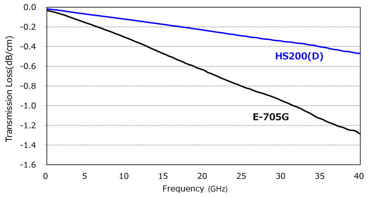
Resonac’s HS200 (D) demonstrates 64% lower transmission loss at 40 GHz than its FC-BGA substrate E-705G.
| Material | HS200(D) | E-705G |
|---|---|---|
| Transmission Loss (dB/cm) @40GHz |
-0.47 (-64%) |
-1.29 (0%) |
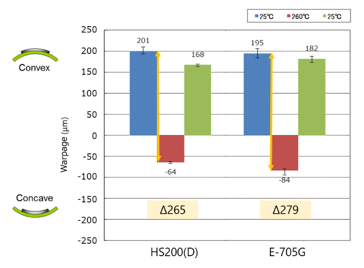
Resonac’s HS200 (D) displays almost the same amount of warpage as its FC-BGA substrate E-705G which is well known for its low CTE.
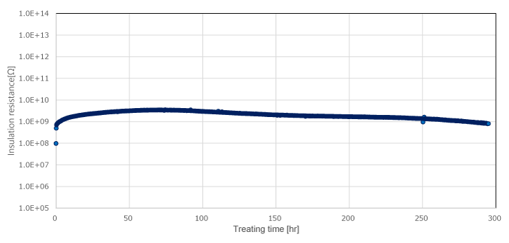
The biased highly accelerated stress test (bHAST) indicates the excellent reliability of Resonac’s HS200 (D).
Update date: 30th January, 2024

Contact Us
Please don't hesitate to contact us if you have any questions.